Summary & Review: Nand to Tetris Part 1
The Nand-to-Tetris course teaches how to build a computer from primitive Nand gates. The second part teaches how to build a fully fledged High level programming language running the Hack computer built in the first part.
The Nand-to-Tetris course is divided into two parts.
Professor Noam Nisan and Shimon Schocken teach the courses.
The first part deals with the hardware ranging from a primitive Nand gate to a CPU.
The course is divided into 6 projects with increasing level of difficulty.
The second part is focused on teaching Software aspect such as high level programming language which runs on the Hack computer.
The Elements of Computing Systems - Building a Modern Computer from First Principles is the referred book for the course. The book is little cryptic to read if you are not doing the online course. For that, I would suggest another book Code: The Hidden Language of Computer Hardware and Software by Charles Petzold which explain the same concepts but in detail.
Overall, the course balances theory with hand-on-practice very well and has right level of difficulty every week.
The second part requires that you know basics of “object oriented programming” as the Jack programming language in the course is similar to Java.
Summary
Week 1
Big picture
The book is divided into 13 chapters and each chapter is equipped with a project. Also, each chapter builds on the previous chapter.
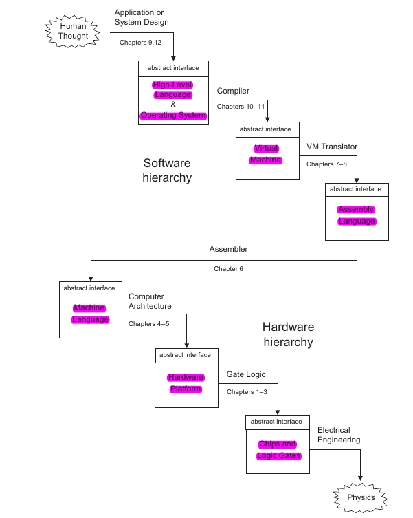
Abstraction
Abstraction is dealing with What is not How-to. Every program is itself an abstraction.
In code System.out.printlin("Hello world"), Every character is an abstraction.
Once we implement the details of an abstraction stage, we forget the implementation and just focus on the abstraction.
For example, we implemented an addition function in stage 1. In stage 2, we just focus on calling the function and not worried about how the function is implemented.
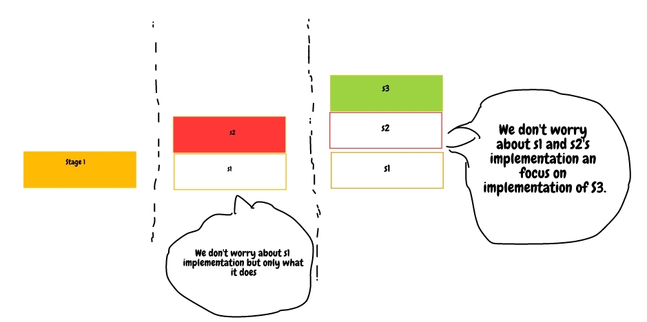 The abstraction is build
 layer by layer
Separation of Concerns
- Once we implement something, we forget about
how-toand just rememberwhat-is
Layers of Abstraction
- Question: Why do we start at Nand gate?.
- Below the level of
Nandgate, there is solid state physics and Electrical engineering. - Computer Science deals with the level of
Nandgate and above.
- Below the level of
The process of building a chip
- Truth Table
- Logic diagram/Chip diagram
- HDL program
- Testing
Example: Building a Xor chip
- Truth Table
| A | B | OUT |
|---|---|---|
| 0 | 0 | 0 |
| 0 | 1 | 1 |
| 1 | 0 | 1 |
| 1 | 1 | 0 |
- Chip diagram
- Use the
karnaught mapto find the number of gates required to build the logical structure.
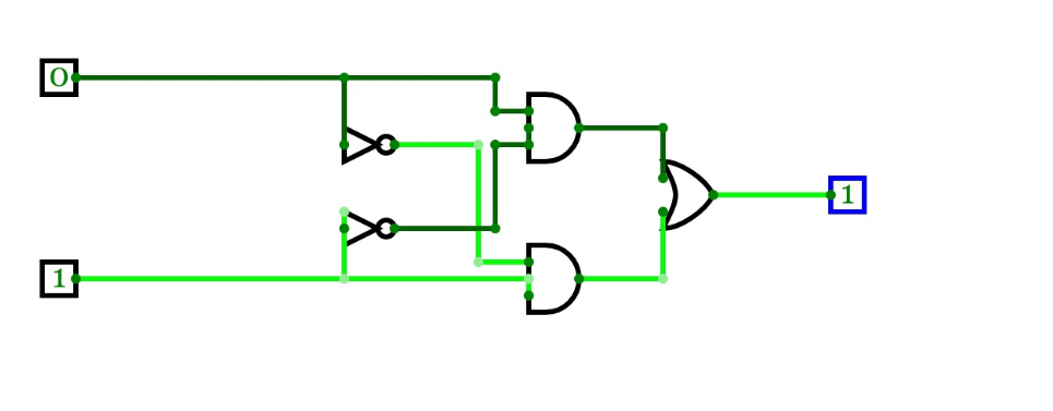
- Use online circuit simulator to verify and visualize the circuit.
- Write a HDL program
/**
 *  Exclusive-or gate: true if either a is true and b is false, or
 *  a is false and b is true; false otherwise.
 */

CHIP Xor {
    IN a, b;
    OUT out;

    PARTS:
    Not (in=a, out=nota);
    Not (in=b, out=notb);
    And (a=a, b=notb, out=x);
    And (a=nota, b=b, out=y);
    Or (a=x, b=y, out=out);
}
- Test Scripts
- Debug, test and complete.
Project week 1
| Gates to build | |
|---|---|
| NAND | AND16 |
| NOT | OR16 |
| OR | MUX16WAY |
| XOR | OR8WAY |
| MUX | MUX4WAY16 |
| DMUX | MUX8WAY16 |
| NOT16 | DMUX4WAY |
| DMUX8WAY |
Boolean Values
The computer works on boolean logic. The boolean consists of only two kinds of state. True and false, 0 and 1
Truth Table
- All possible values of Input and Output.
Boolean Identities
Commutative | (x and y) = (y and x) | (x or y) = (y or x) | |||||||
Associative | (x and (y and z))= ((x and y) and z) | (x or(y or z))= ((x or y) or z) | |||||||
Distributive | (x AND (y OR z) = ((x AND y )OR(x AND z ) | (x OR (y AND Z)) = ((x OR y )AND(x OR z ) | |||||||
DeMorgan | NOT(x AND y) = NOT(x) OR NOT(y) | NOT(x OR y) = NOT(x) AND NOT(y) |
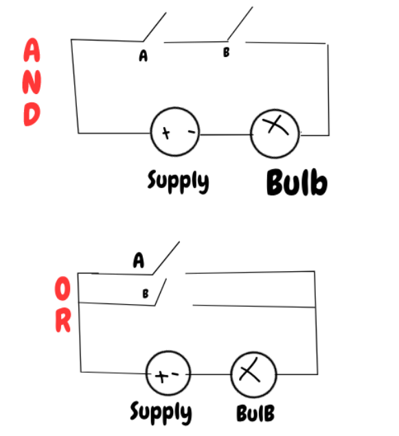
Why Nand Gate
- The
Nandgate can replaceNOT,AND,ORgates.
Building Not from NAND
- NOT gate truth table.
| in | OUT |
|---|---|
| 0 | 1 |
| 1 | 0 |
- A NAND gate with a single source connected to both inputs resembles a NOT gate.
| A | B | OUT |
|---|---|---|
| 0 | 0 | 1 |
| 1 | 1 | 0 |
x NAND y = NOT(x AND Y)
x NAND x = NOT (x AND x)
Here x AND x = x
so,
X NAND x = NOT(x)

Similarly, NAND gate can be utilized to construct AND, OR gates.
Interface vs Implementation
- There must be one interface but there can be many implementations.
Circuit Implementations
- We don’t focus on circuit design in this course.
- AND, OR gates implementation at circuit level
HDL guide
- HDL is
hardware description language. - Readability matters so name internal wires sensibly.
- functional language.
- You can write code in any order.
Multi-bit Bus
- Multi-bit bus allows to manipulate a group of bits together.
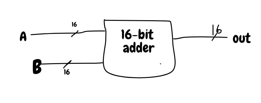
- It convenient to think of
16 bitas an array or group. (single unit)- However, its implemented as 16 wires.
- So
A+Bis basically addition of two16-bitnumbers.
- The grouping is called a
bus.
Multiplexer
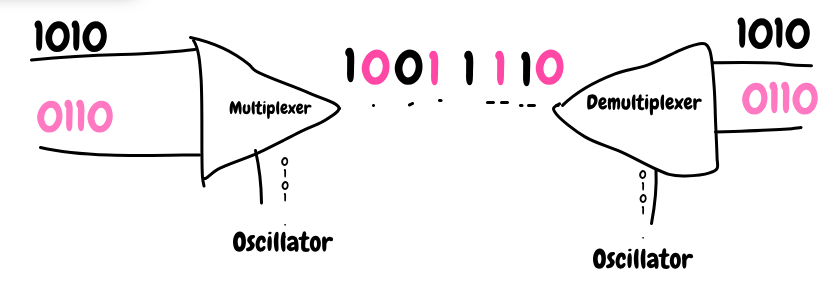
- Multiplexer transmit two sources on a single line.
- The source and destination does not need to synchronize with master clock.
- Each can have their own oscillator.
16Bit 4 way Multiplexer
4 wayimplies that there are 4 input sources.16 bitindicates that each input is16 bit.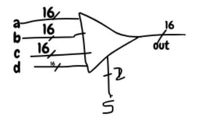
Number representation
- 8 bit = 2^8 bits = 256
- we need to represent range of positive and negative numbers.
Decimal to Binary
99 =>   64 - 32 - 16 - 8  - 4 - 2  -  1
       _________________________________
       |64 + 32|                 |    |
        ------                  |     |
          |                     |     |
         96 -------------------|2|    |
                                |     |
                                98---|1|
                                      |
                                     99
        ________________________________
        1 -  1 -  0 -  0  -  0 - 1 -  1
        ________________________________
Week 2
The whole point to represent number is to manipulate it.
Binary Addition
The addition is similar to decimal
    1 1 1 1
    0 0 0 1
    -------
 1  0 0 0 0    --> The sum
 ^  -------
 |
 This is the carry bit which is ignored if overflow.
overflow
Computer ignores the overflow bit as it cannot be stored.
-> Example: Suppose we add two 8 bit numbers. Then, if addition produces a 9 bit, then it is ignored as we cannot store it in an 8-bit output.
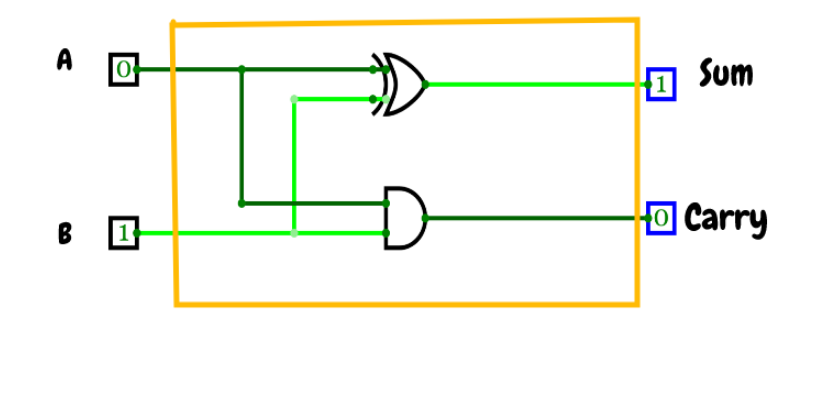
Half Adder
A half adder has two inputs and adds them providing sum and carry.
| A | B | Sum | Carry |
|---|---|---|---|
| 0 | 0 | 0 | 0 |
| 0 | 1 | 1 | 0 |
| 1 | 0 | 1 | 0 |
| 1 | 1 | 0 | 1 |
The sum column output is same as XOR
The carry column output is same as AND
Full Adder
| A | B | C | Sum | Carry |
|---|---|---|---|---|
| 0 | 0 | 0 | 0 | 0 |
| 0 | 0 | 1 | 1 | 0 |
| 0 | 1 | 0 | 1 | 0 |
| 0 | 1 | 1 | 0 | 1 |
| 1 | 0 | 0 | 1 | 0 |
| 1 | 0 | 1 | 0 | 1 |
| 1 | 1 | 0 | 0 | 1 |
| 1 | 1 | 1 | 1 | 1 |
Sum
= $ \overline{\rm a}\overline{\rm b}c+ $ $ \overline{\rm a}b\overline{\rm c}+ $ $ a\overline{\rm b}\overline{\rm c}+ $ $ abc $
= $ \overline{\rm a}[\overline{\rm b}c+b\overline{\rm c}]+ $ $ a[bc+\overline{\rm b}\overline{\rm c}] $
Carry
= $\overline{\rm a}bc+a\overline{\rm b}c+ab\overline{\rm c}+abc$
= $c[\overline{\rm a}b+a\overline{\rm b}] +ab[c+ \overline{\rm c}]$
=$ab+c[\overline{\rm a}b+a\overline{\rm b}] $
Tips
- Use half adder to implement full adder.
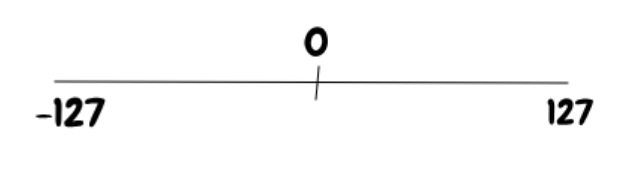
Negative numbers
Negative number are represented using 2's complement.
| Number | $2^2$ | $2^1$ | $2^0 $ | $2^0$ |
|---|---|---|---|---|
| 0 | 0 | 0 | 0 | 0 |
| 1 | 0 | 0 | 0 | 1 |
| 2 | 0 | 0 | 1 | 0 |
| 3 | 0 | 0 | 1 | 1 |
| 4 | 0 | 1 | 0 | 0 |
| 5 | 0 | 1 | 0 | 1 |
| 6 | 0 | 1 | 1 | 0 |
| 7 | 0 | 1 | 1 | 1 |
| 8 | 1 | 0 | 0 | 0 |
| 9 | 1 | 0 | 0 | 1 |
| 10 | 1 | 0 | 1 | 0 |
| 11 | 1 | 0 | 1 | 1 |
| 12 | 1 | 1 | 0 | 0 |
| 13 | 1 | 1 | 0 | 1 |
| 14 | 1 | 1 | 1 | 0 |
| 15 | 1 | 1 | 1 | 1 |
ALU
ALU is arithmetic and logical unit. Arithmetic functions are addition, subtraction, division, multiplication. Logical: And, Xor, OR
- Que: What operations to implement in hardware.
- Depends on tradeoff b/w hardware and software.
Design of HACK ALU
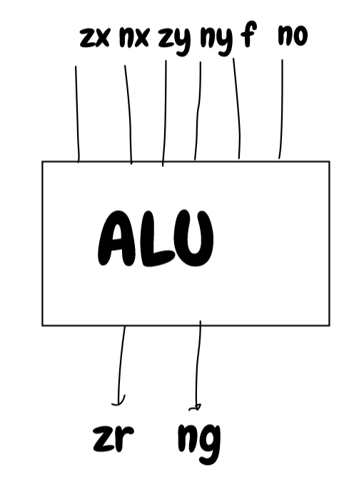
| zx | nx | zy | ny | f | no | out | ||||||||
|---|---|---|---|---|---|---|---|---|---|---|---|---|---|---|
| y,zx=1 | ||||||||||||||
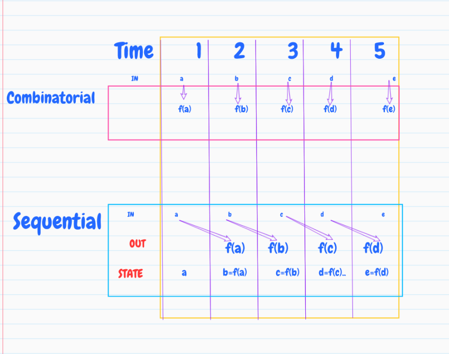
Week 3: Sequential Logic
Sequential logic includes the concept of time. Sequential logic allows to
- Reuse hardware
- Output is function of previous output.
Time
What do we want time for.
- Primarily for reusing hardware.
- State
- Remember things.
- Eg. Counter, memory.
- Speed: We need to make sure that we don’t ask computer to perform beyond its max speed.
The Clock
- Analog time is continuous.
- We convert it to discrete time.
- Then, we adjust time cycle to compensate for electrical delays.
Electrical signal delay
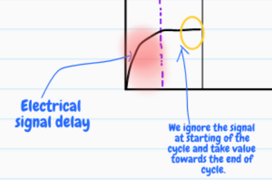
- Voltage is
continuous(like wave).- It takes time to change.
- So, we ignore the signal towards start of the cycle.
- Output takes even more time.
- Due to the physical gates delay.
- To counter these, the clock cycle speed is set to allow enough time for both the scenarios.
Combinational vs Sequential
- Combinational output depends on input.
- Sequential output depends on previous output(state).
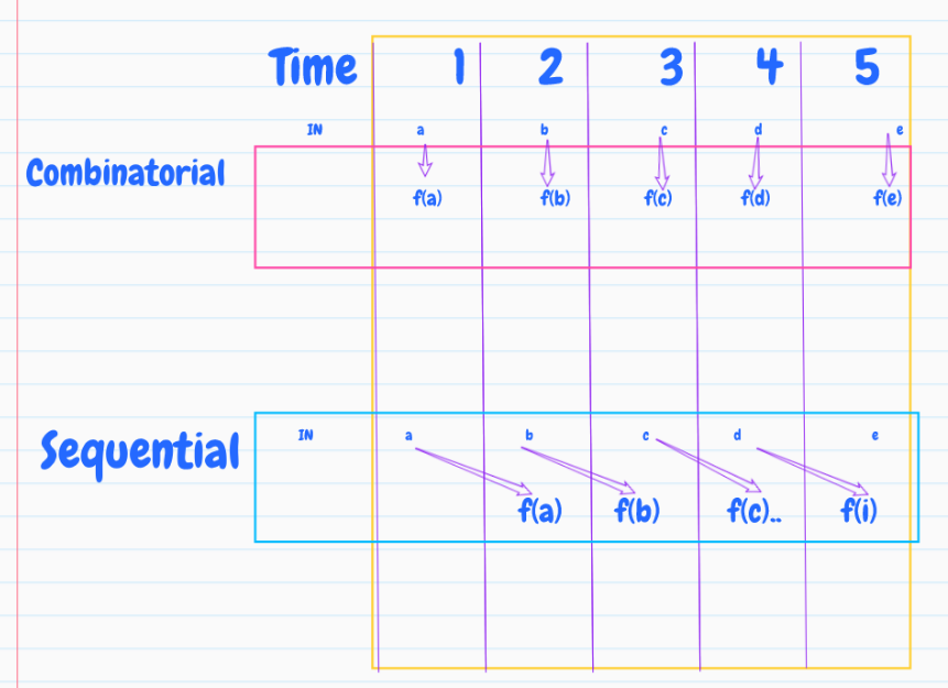
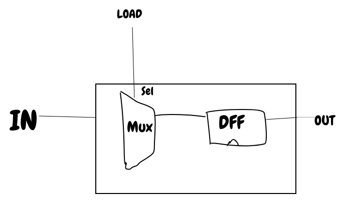
Clocked data flip flop
SR latchis used to remember previous state.- It’s built from two
Nand gates.
- It’s built from two
- The previous state can be 0 or 1.
- We need to flip the state.
1 Bit Register
load(t-1) -> out(t) = in(t-1)
else       -> out(t) = out(t-1)
Ram
- Ram is a sequence of
n-addressableregisters.
At any time, only 1 register is selected.
How to determine address.
- The address bit helps to determine the address.
- k=$log_2{n}$
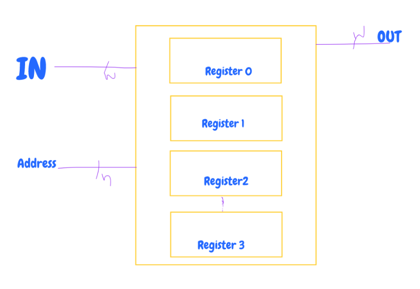
16 BIT RAM chip family
| Name | n | k |
|---|---|---|
| RAM8 | 8 | 3 |
| RAM64 | 64 | 6 |
| RAM512 | 512 | 9 |
| RAM4K | 4096 | 12 |
| RAM16K | 16384 | 14 |
- RAM is called Random access memory as you can access random register in same time.
Counter
- A program counter is useful for 3 scenarios.
- Increment instruction
- Go to a specific instruction(JUMP)
- Reset to 0.
Control settings
- fetch: fetch the first instruction -> pc=0
- goto: goto
ninstruction -> pc=n
- goto: goto
- next: fetch the next instruction -> pc++
Reset = 1, out(t+1) = 0
Inc = 1, out(t+1) = out(t) + 1
Load = 0, Inc = 0 (default), out(t+1) = out(t)
Ram8
- The selector has 3 bits.
| s2 | s1 | s0 |
|---|---|---|
| 0 | 0 | 0 |
| 0 | 0 | 1 |
| 0 | 1 | 0 |
| 0 | 1 | 1 |
| 1 | 0 | 0 |
| 1 | 0 | 1 |
| 1 | 1 | 0 |
| 1 | 1 | 1 |
- Utilize DMux to distribute load to the right register using
address bits.
Similarly, Ram64, Ram512 are constructed.
Week 4
Machine language is low level language.
- It is the interface between hardware and software.
Universality
Alan Turing theorized a machine with notion of what can be computed.
Universal Turing machine - can act like any other Turing machine given the correct program.
- Mnemonics
- Symbolic machine language.
- Example.
Add R1whereAddis mnemonic
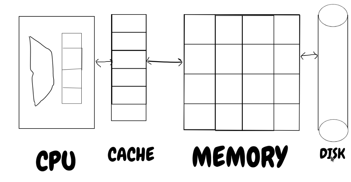
Memory Hierarchy
- Accessing big memory for saving each computation is time consuming.
- Long Address
- time consuming due to data transfer from CPU to memory and vice versa.
The solution is Memory hierarchy which has faster memory such as registers near the CPU and stores the computation results there,
Flow Control
- conditional jump
- The jump is based on the condition.
- For eg. Jump if R1 is not equal to 0
- Unconditional Jump.
Hack Computer: Hardware
Screen
- Screen is assigned a specific area in the memory called
screen memory map. 
- Physical screen is continuously refreshed many times to update the content.
How does the program show output
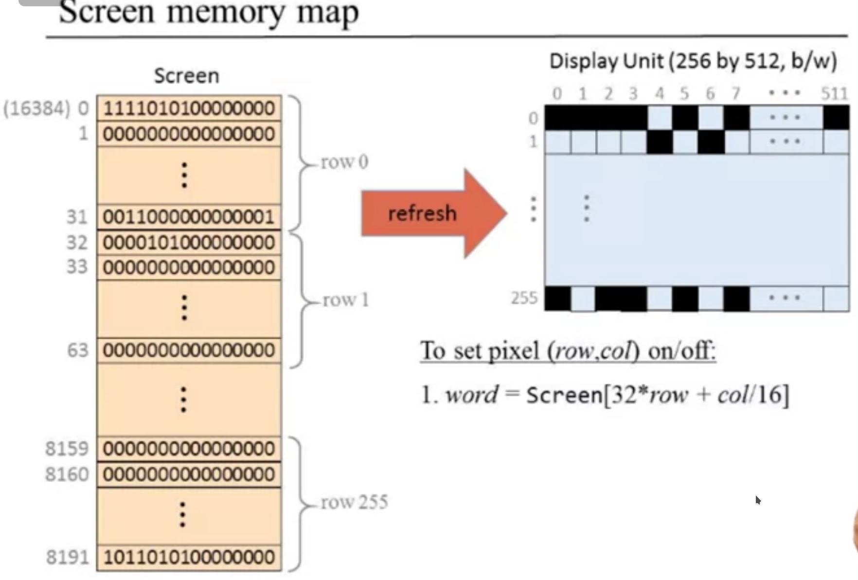
- The software driver for the screen updates the screen memory map area.
Keyboard
- Pressed key’s scan code travels to
keyboard memory map.- It is a 16 bit register.
NOP Slide attack
- The program if not terminated can run instructions put by a hacker.
How to terminate properly.
- Computers never stand still.
- So, to end a program, put an infinite loop at the end of the program.
Built-in symbols
- We use symbols in machine language to make it easier to read.
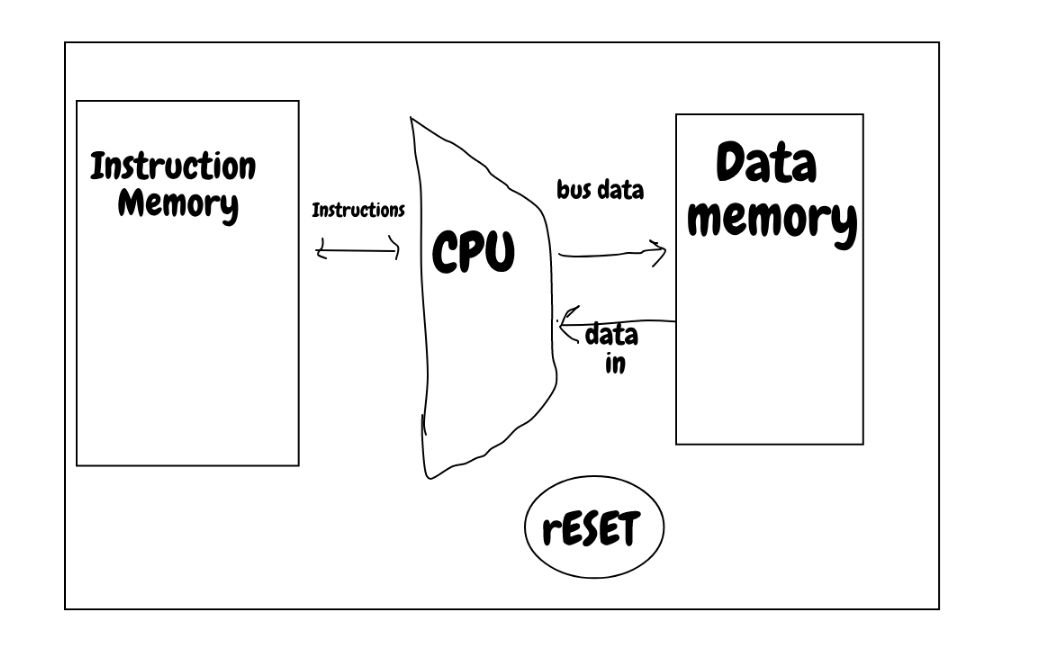
Week 5: Computer Architecture
Data flow
- 3 types of information passes through the system.
- Data
- Address
- Control
Fetch Execute cycle
- There are two kinds of architecture.
- Harvard architecture has program and data separately.
- So, we can fetch and execute in the same cycle.